In many semiconductor industry news stories, you often hear about 8-inch or 12-inch fabs. Why are they named after their size? What is the name of the wafer? How hard is it to make a large wafer? Today, xiaobian will discuss with you to understand.
Wafer, in fact, is the basis of all kinds of computer chips, is the manufacture of IC basic raw material. As we all know, the main raw material of IC is silicon, so the corresponding is silicon wafer. Because of its circular shape, it is called a wafer. After that, various circuit components are fabricated on silicon wafers to become integrated circuit products with specific electrical functions.
What people do not know is that the rise of Silicon Valley in the United States also started from the semiconductor industry, hence the name silicon Valley.
Silicon is a common substance, in nature in the form of silicate or silica is widely found in rocks, gravel, and the earth's crust surface of inexhaustible silica. Silica ore is extracted by electric arc furnace, chlorinated by hydrochloric acid, and distilled into high purity polysilicon, its purity up to 99.999999999%. Its manufacture can be summarized into three basic steps: silicon extraction and purification, monocrystalline silicon growth, wafer forming.
Is to use these rocks or gravel, after many purification, high temperature shaping, and then using the way of rotary stretching, into a cylindrical, monocrystalline silicon ingot. Individual ingots weigh about 100 kilograms.

A single crystal silicon ingot is the original form of a wafer, which is cut horizontally to create cylindrical silicon wafers that are polished to a mirror-like surface.
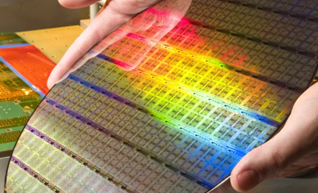
We often hear about the size of a fab, such as an 8 - or 12-inch fab. What does that size really mean? In fact, this 8 "or 12" is actually the diameter of the wafer. The larger the diameter, the more difficult the manufacturing process, and the better technology the fab has. As chips get smaller, thousands of them can be cut from a single wafer.
There is also scaling, which reduces the size of transistors and wires, both of which can produce more silicon grains on a single wafer, improving quality and reducing costs. Among these 8-inch and 12-inch wafers, 12-inch wafers have higher capacity and are currently the mainstream of the market.
Some known as Fabless chip manufacturers, is a professional engaged in design, development and sales of chips such as qualcomm, huawei, broadcom, spreadtrum, etc., but they do not have their own factories, all manufacturing operations need to package to the professional production factory, which is called the Foundry, foundries, such as TSMC, smic and so on. Currently, TSMC is the world's largest contract chipmaker, with a market share of about 67 percent.